
Avalanche transit time devices
In this blog, we will explore and learn about avalanche transit time devices -
i) What is the IMPATT diode?
a) Construction and operation.
b) Advantages & Disadvantages.
c) Applications.
Some microwave diodes exhibit negative resistance having a delay between voltage and current in an avalanche together with transit time through the material. These devices are called avalanche transit time devices. These types of devices use carrier impact ionization. Avalanche transit time devices are of three types -
(i) IMPATT diode
(ii) TRAPATT diode
(iii) BARITT diode.
IMPATT Diode
IMPATT Diode Construction - The construction of IMPATT diodes is shown in Fig. and the equivalent circuit of IMPATT diode is shown in Fig. In the IMPATT diode, the magnitude of negative resistance R_{a} is less than the reactance X_{d} so that the chip impedance of the IMPATT diode is capacitive, For a 10 GHz IMPATT diode chip external epitaxy inductive wire has a value of 0.6 mH and a bulk capacitance of 0.3 pF.
Operation of IMPATT Diode - The device that exhibits negative resistance for D.C. will also exhibit it for A.C. Negative resistance is defined as the property of the device that causes the current through it to be 180° out of phase with the voltage across it. This kind of negative resistance is exhibited by the IMPATT diode. As shown in Fig. IMPATT is a diode, the junction being between the p+ and n+ layers.
When an extremely high voltage gradient (400 kV/em) is applied to the IMPATT diode eventually results in a very high current A normal diode would very quickly break under these conditions but IMPATT is constructed such that it will withstand these conditions. Due to high potential gradient back biasing the diode causes a flow of minority carriers across the junction.
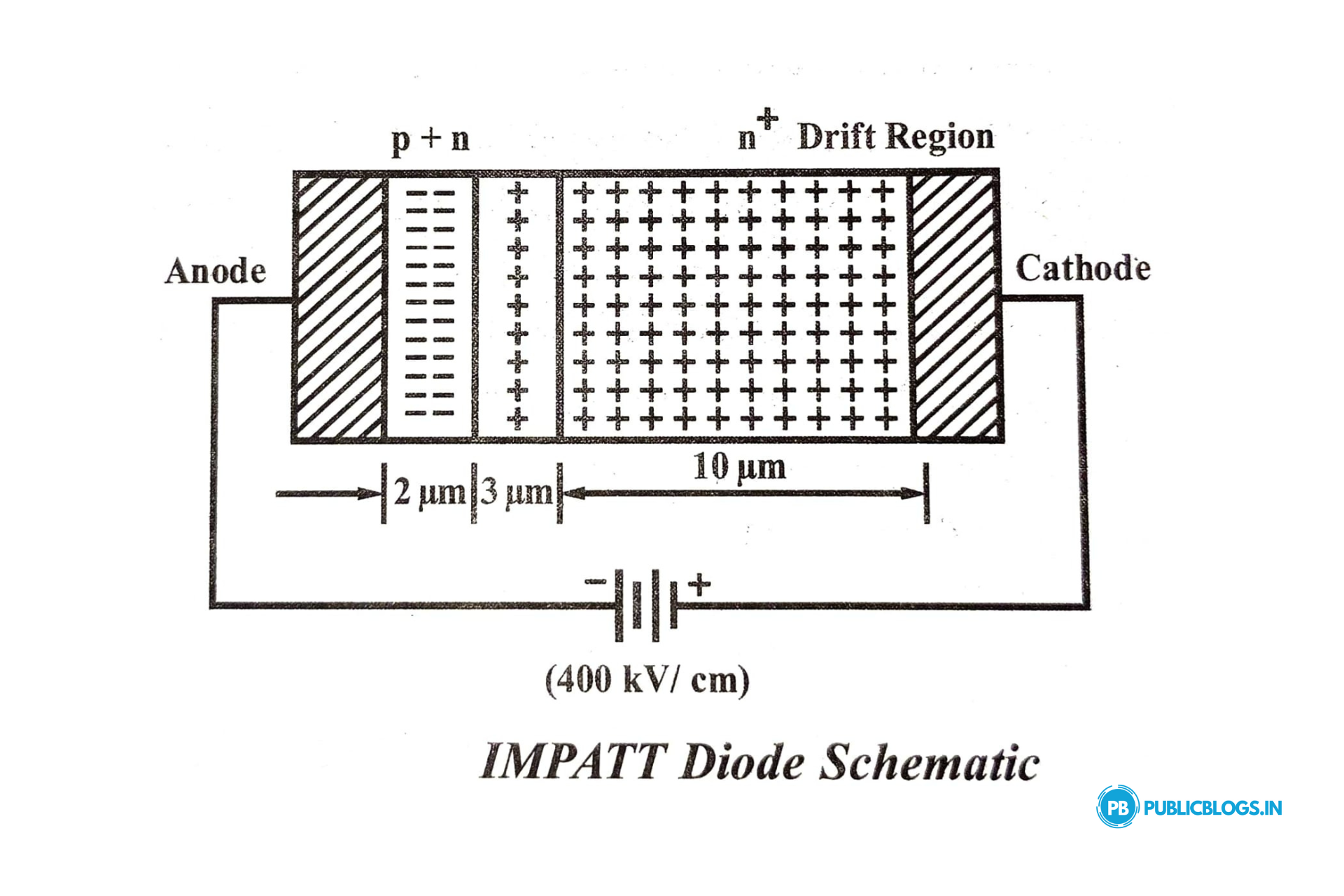 Let us take the application of RF A.C. voltage superimposed on the top of the high D.C. voltage. When the velocity of electrons and holes increases due to this reason electrons and holes by knocked out of the crystal structure by so-called impact ionization. At the junction, these extra carriers continue the process.
This process takes time so that the current pulse is maximum at the junction and occurs at the instant when RF voltage across the diode is zero and going negative. Because of this, we achieved a 90° phase shift or phase difference between voltage and current. The current pulse shown in the figure is situated at the junction.
It moves towards the cathode due to applied reverse bias at a drift velocity depending on the presence of a high D.C. field but does not stay A there. The time taken by the pulse to reach the cathode depends on its velocity and the thickness of the highly doped 'n+' (charges) layer.
The thickness is adjusted so that the time taken for the current pulse to move from V = 0 position to V = negative maximum of the RF cycle is exactly 90°. Therefore voltage and current are 180° out of phase.
Disadvantages of IMPATT Diode -
(i) The tuning range is not as good as Gunn diodes.
(ii) It is very noisy because an avalanche is a noisy process.
(iii) Noise figures of the IMPATT diode being 30 dB are not as good as the Klystron/Gunn diode.
Applications of IMPATT Diode -
(i) IMPATT diodes are used for negative resistance amplification -
(a) High Q IMPATTs are used in police radar, intrusion alarm
(b) Low Q IMPATTs are useful in FM telecommunication transmitters and CW Doppler radar transmitters.
(ii) IMPATT diodes are used as microwave oscillators -
(a) Parametric amplifier pumps
(b) Receiver local oscillator
(c) Microwave generator
(d) Modulated output oscillator
TRAPATT Diode
Basically, a TRAPATT diode made from the TRAPATT is a high-efficiency microwave generator that is capable of working at several hundred MHz to several GHz. It is typically a p+-n-n+ silicon or GaAs structure, as shown in Fig.

The configuration of the TRAPATT diode in a circuit is shown in Fig. TRAPATT is a reverse-biased diode with a tuning circuit consisting of L and C. It is mounted at one end of a transmission line.
find where,
L = Packaged inductance
C = Epitaxed bulk capacitance.
Operation- A high field avalanche zone propagates by the diode and the depletion region is filled by dense plasma of electrons and holes d which become trapped in the low field region behind the zone. In Fig. we have to see that AB shows charging, BC shows plasma formation, and DE shows plasma extraction. EF shows residual extraction and FG shows charging.
The electric field is uniform at point a throughout the sample and the magnitude of this field is large but less than the value required for avalanche breakdown At a charge carrier due to thermal generation results in charging of the diode as a linear capacitance AB driving the magnitude of electric field above the breakdown voltage. The practical current exceeds the external current if a sufficient number of carriers are generated. Because of voltage decrease (BC) electric field is depressed throughout the depletion region.
During this time the electric field is sufficiently large for the avalanche to continue because of this dense plasma of electrons and holes is produced. Some electrons and holes drift out the ends of the depletion layer so the field is depressed. The voltage decreases to point D. A long time is needed to remove the plasma. At point E the plasma is removed, but the residual charge of electrons remains at one end of the depletion layer and a residual charge of holes at the other end.
If the residual charge is removed. Then voltage increases from point E to F, so that at point F, all the charge is removed and this charge must be greater or equal to supplied by the external current. Otherwise, the voltage will exceed that at point A. The diode charges up again as a capacitor at the point from F to G.
BARITT Diode
Barrier-injected transit time diodes (BARITT) are the latest addition to the family of active microwave devices. They consist of long drift regions as like to those of IMPATT diodes. However, the carrier traversing the drift region of BARITT diodes is produced by minority carrier injection from forward-biased junctions instead of being extracted from the plasma of an avalanche region. These diodes are much less noisy than IMPATTs with noise figures as low as 15 dB.
The main disadvantages of BARITT are narrow bandwidth and power output limitation. These devices are an improved version of IMPATT devices. IMPATT devices use impact ionization techniques which are very noisy. To obtain low noise figures, impact ionization is avoided in BARITT diodes. Minority injection is provided by punch-through of the intermediate region (depletion region).
This process differs in the sense that it has lower noise compared to impact ionization responsible for current injection in an IMPATT diode. In a BARITT device, the negative resistance is achieved on account of the drift of the injected holes to the collector end of the diode, made of p-type material. The constructional details of a typical BARITT device are shown in Fig.

The necessary requirement for a BARITT device is that the intermediate drift region be entirely depleted to cause a punch through the emitter-base junction without causing the available breakdown of the base-collector junction.
In the case of a m-n-m BARITT diode, the Ps-Si Schottky barrier contacts metals with an n-type silicon wafer in between a rapid rise in current with applied voltage (above 30V) because of the thermionic hole injection into the semiconductor as shown in Fig.
Conclusion -
In this, we learn about avalanche transit devices, what they are, what are the applications of them, and what are the types of them. We have also learned about the IMPATT diode. what is it, what are the applications of it, what are the major advantages and disadvantages of it. We have also learned about the TRAPATT diode. what is it, what are the applications of it, what are the major advantages and disadvantages of it.
We have also learned about the BARITT diode. what is it, what are the applications of it, what are the major advantages and disadvantages of it. I hope you enjoy this blog learn new things and gain a lot of knowledge about avalanche transit devices.
Do you dream of turning your thoughts and words into income ? join us now and become blogger now.


0 Comments
Leave a Comment